Introduction
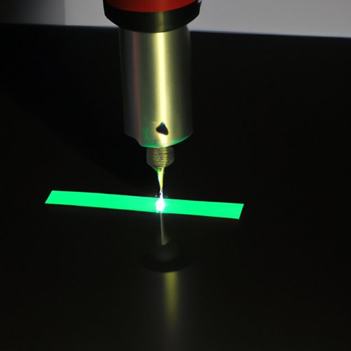
Scanning Probe Microscopes (SPMs) are a type of microscope that uses a probe to scan a surface in order to obtain an image of its features. The probe is moved across the surface of the sample and records information about the topography or other relevant characteristics. This information is then processed to create an image of the surface. SPMs have become increasingly important tools for researchers in fields such as nanotechnology, biophysics, and materials science.
The purpose of this article is to explore the technology used behind Scanning Probe Microscopes (SPMs). We will look at how they work, their components, and the latest advances in Scanning Probe Microscopy (SPM). By the end of this article, readers should have a better understanding of the technology behind SPMs and be able to make informed decisions when considering their use.
Exploring the Science Behind Scanning Probe Microscopes
Before we dive into the technology used behind SPMs, let’s first take a look at what they are and how they work. A Scanning Probe Microscope is a type of microscope that utilizes a probe to scan a surface in order to obtain an image of its features. The probe is moved across the surface of the sample and records information about the topography or other relevant characteristics. This information is then processed to create an image of the surface.
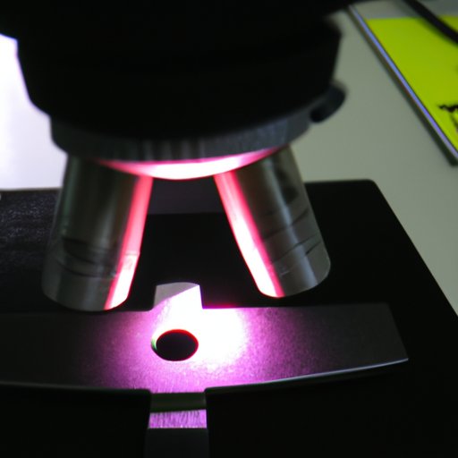
There are several different types of SPMs, each designed to measure different properties of a sample. Atomic Force Microscopes (AFMs) are used to measure force interactions between the probe and the sample, while Scanning Tunneling Microscopes (STMs) measure the tunneling current between the probe and the sample. Other types of SPMs include Magnetic Force Microscopes (MFMs), Scanning Near-field Optical Microscopes (SNOMs), and Photoemission Electron Microscopes (PEEMs).
An Overview of the Technology Used in Scanning Probe Microscopes
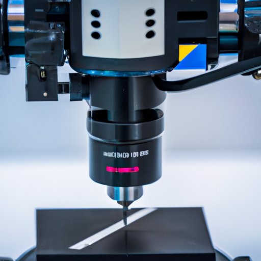
Now that we have a basic understanding of what SPMs are and how they work, let’s take a closer look at the technology used in them. SPMs are composed of both hardware and software components. The hardware components include the probe, cantilever, and piezoelectric materials, while the software components consist of the control system, data analysis software, and image processing software.
The probe is the most important component of an SPM. It is usually made of a sharp tip, which can range in size from a few nanometers to a few micrometers. The cantilever is a thin strip of metal or plastic that is attached to the probe. It is used to measure the forces exerted on the probe by the sample. Piezoelectric materials are materials that can produce an electric voltage when subjected to mechanical stress. These materials are used to move the probe across the surface of the sample.
The control system is responsible for controlling the movement of the probe and the cantilever. It also processes the signals received from the probe and cantilever and sends them to the computer for data analysis. Data analysis software is used to analyze the data collected by the probe and cantilever. Finally, image processing software is used to create images of the sample based on the data collected by the probe and cantilever.
How Scanning Probe Microscopes Work: A Closer Look at the Technology
In addition to the hardware and software components of an SPM, there are also certain physical principles involved in the operation of an SPM. The most important of these are the atomic force and tunneling effects. The atomic force effect occurs when the probe comes into contact with the sample and the forces between them cause the cantilever to bend. The tunneling effect occurs when electrons move between the probe and the sample due to a voltage applied to the probe.
Data acquisition and analysis are also important components of SPMs. Data is acquired by measuring the displacement of the cantilever as it moves across the surface of the sample. This data is then analyzed to create an image of the sample. Image processing techniques such as Fourier transform are often used to enhance the resolution of the image.
A Guide to the Design and Operation of Scanning Probe Microscopes
When designing and operating an SPM, it is important to consider a number of factors. System design considerations include the type of probe, the type of sample to be examined, and the environment in which the SPM will be operated. Operating parameters and techniques must also be taken into account, such as the speed of the probe, the force applied to the sample, and the duration of the scan.
It is also important to consider the safety of the operator. Proper safety precautions must be taken when operating an SPM, including wearing protective clothing and eye protection. Additionally, it is important to follow the manufacturer’s instructions for the proper use and maintenance of the SPM.
The Latest Advances in Scanning Probe Microscopy
The field of Scanning Probe Microscopy has seen tremendous advances in recent years. Automation and robotics have enabled SPMs to operate more accurately and efficiently. High resolution imaging and spectroscopy techniques have been developed, allowing for the study of samples at the nanoscale. Newer SPMs can also be used to measure electrical, magnetic, and optical properties of samples.
These advances have opened up new possibilities for researchers in fields such as nanotechnology, biophysics, and materials science. SPMs are now being used to study a wide range of materials, from organic molecules to semiconductors. They are also being used to study biological systems, such as cells and proteins.
Examining the Components of a Scanning Probe Microscope
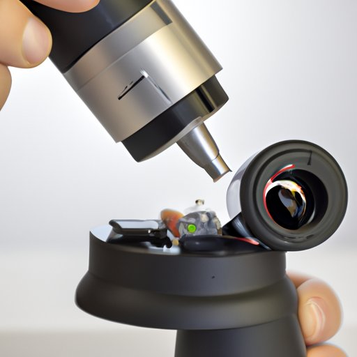
Let’s take a closer look at the components of an SPM. Probes and cantilevers are the two main components of an SPM. Probes come in a variety of shapes and sizes and can be made of a variety of materials, such as silicon, tungsten, and carbon nanotubes. Cantilevers are typically made of metal or plastic and are used to measure the forces exerted on the probe by the sample.
Piezoelectric materials are also used in SPMs. These materials can generate an electric voltage when subjected to mechanical stress. This voltage can be used to move the probe across the surface of the sample. Piezoelectric materials are also used in the construction of probes, cantilevers, and other components of SPMs.
Conclusion
In conclusion, this article has explored the technology used behind Scanning Probe Microscopes (SPMs). We have looked at the different types of SPMs, the physical principles involved, the hardware and software components, the latest advances in SPM, and the components of an SPM. By understanding the technology behind SPMs, researchers can make informed decisions when considering their use.
The use of SPMs has enabled researchers to study a wide range of materials at the nanoscale. Their ability to measure electrical, magnetic, and optical properties of samples has made them invaluable tools in fields such as nanotechnology, biophysics, and materials science. With the continued advancement of SPM technology, the possibilities for research are endless.
(Note: Is this article not meeting your expectations? Do you have knowledge or insights to share? Unlock new opportunities and expand your reach by joining our authors team. Click Registration to join us and share your expertise with our readers.)